 Tiếng
Việt
Tiếng
Việt
 Tiếng
Anh
Tiếng
Anh
 Tiếng
Nhật
Tiếng
Nhật




 Tiếng Anh

What are the main stages of the PCB manufacturing process?

Printed circuit boards (PCBs) are used in almost every electronic device, from chargers and household appliances to industrial control systems and transportation equipment. To produce a complete circuit board, the product goes through multiple manufacturing stages, which can generally be divided into two major phases: bare PCB fabrication and PCBA assembly. Each phase consists of various processes involving design, circuit pattern formation, component placement, soldering, protection, inspection, and finishing. Together with CNC VINA, let’s explore the PCB manufacturing process and the equipment commonly used at each stage.
1. What is a PCB? Common types of PCBs
A PCB (Printed Circuit Board) is a circuit board made from an electrically insulating substrate with copper conductive traces that connect electronic components and transmit electrical signals between them. Depending on the design, a PCB may contain one or multiple conductive layers, which are patterned according to the circuit layout and surface-treated to meet the assembly, soldering, and application requirements of the final product. A PCB that has been fabricated but does not yet have any components mounted on it is commonly referred to as a bare PCB. Once electronic components are mounted onto the board and the required assembly, soldering, and inspection processes are completed, the finished product is known as a PCBA (Printed Circuit Board Assembly). Therefore, the manufacturing process of a complete electronic circuit board generally includes both PCB fabrication and PCBA assembly.
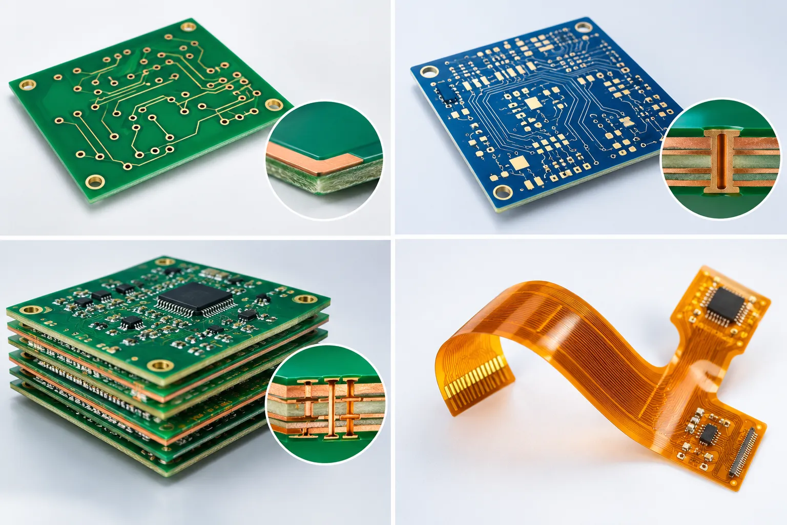
Some common types of PCBs include:
Single-sided PCB
A single-sided PCB has one main conductive copper layer on one side of the substrate. Its relatively simple structure makes it a cost-effective solution for circuits that do not require a high routing density, such as certain power supplies, lighting products, and household electronic devices.
Double-sided PCB
A double-sided PCB has conductive copper layers on both sides of the substrate. The two sides can be electrically interconnected through plated-through holes or vias, providing more space for routing traces and placing components compared with a single-sided PCB. This structure is widely used in various control systems and industrial electronic devices.
Multilayer PCB
A multilayer PCB consists of multiple conductive layers stacked and laminated into a single integrated structure. These layers are interconnected through a system of holes and vias according to the circuit design, enabling higher routing density and supporting more complex electronic circuits.
Flexible PCB
A flexible PCB (FPC – Flexible Printed Circuit) uses a flexible substrate that can bend instead of the rigid board structure used in conventional PCBs. This type of circuit is suitable for devices with limited installation space or applications requiring flexible connections, such as smartphones, cameras, displays, and other compact electronic devices. Depending on the PCB type, materials used, and product requirements, the bare PCB fabrication process may vary. Once fabrication is complete, the PCB proceeds to the component assembly stages to form a PCBA.

Overview of the PCB manufacturing process
Depending on the PCB structure, materials used, and product requirements, the actual manufacturing process may vary. However, when considering the complete production chain of an electronic circuit board, the processes can generally be divided into two main groups: bare PCB fabrication and PCBA assembly.
| Stage | Main processes |
|---|---|
| Bare PCB fabrication | Design → material cutting → drilling → plating → circuit pattern formation → solder mask → surface treatment → inspection |
| SMT assembly | Solder paste printing → component placement → reflow soldering |
| THT assembly | Through-hole component insertion → soldering |
| PCB protection | Adhesive dispensing → coating → potting |
| Finishing | Board separation → cutting → laser marking |
| Inspection | Visual inspection → AOI → ICT/FCT → final inspection |
PCB fabrication focuses on producing a bare board with conductive paths and other structures required by the design. The PCB can then proceed to the PCB assembly stage, where components are mounted, soldered, protected, and inspected to produce a complete circuit board assembly.
Bare PCB fabrication stage
The bare PCB fabrication stage transforms copper-clad substrate material into a PCB with conductive paths, connection holes, and the necessary protective layers. Depending on the production scale and manufacturing model, these processes are typically carried out at a dedicated PCB fabrication plant or production area before the boards are transferred to PCBA assembly.
Design and production file generation
Before manufacturing begins, engineers design the circuit using specialized software and prepare the data required for fabrication. Production data typically includes Gerber files for individual layers and related information, together with drill data specifying the locations and dimensions of the holes to be machined. Before production, the data may be reviewed according to Design for Manufacturing (DFM) principles to identify design features that could create difficulties during fabrication. This helps reduce the risk of defects during mass production.
Material cutting and hole drilling
Copper-clad sheets are prepared and cut to dimensions suitable for the production panel. CNC drilling machines process holes according to the design data, including through holes, tooling holes, and holes used for interlayer connections, depending on the PCB structure. Drilling accuracy directly affects hole positioning, component assembly, and the quality of electrical connections formed in subsequent processes.
Copper plating of through holes
For PCBs that require interlayer connections, the hole walls are treated and plated with copper to form conductive paths according to the design. The copper layer on the hole walls connects the conductive layers of the PCB through plated-through holes and vias. The quality of this process has a direct impact on connection stability and the long-term reliability of the circuit board during operation.
Circuit pattern formation and etching
The circuit pattern is transferred onto the PCB surface through imaging and material-processing steps appropriate to the manufacturing technology. Copper areas that are not part of the circuit pattern are removed, leaving the conductive traces, pads, and other structures required by the design. For multilayer PCBs, the inner circuit layers may be fabricated separately before being laminated together with other material layers to form the multilayer structure. The board then proceeds through the corresponding machining and surface treatment processes.
Solder mask application and legend printing
Solder mask is a protective coating applied to the PCB surface. It is commonly green, although other colors may be used depending on product requirements. The coating protects copper areas that are not intended for soldering, helps limit environmental exposure, and reduces the risk of solder bridges forming between adjacent conductive areas. A silkscreen layer can then be printed onto the board to indicate component locations, symbols, logos, product codes, and other identification information.
Pad surface treatment
Solderable pads undergo surface treatment to protect the underlying copper and meet the soldering requirements of the assembly process. Common surface finishes include HASL, ENIG, and OSP. The choice of surface finish depends on factors such as soldering requirements, PCB materials, storage life, operating environment, and product characteristics.
Profiling and electrical testing
After the main fabrication processes are completed, the PCB may be machined to its designed profile using a router, milling process, or another suitable method. For panels using V-cut scoring, V-shaped grooves are created in advance to facilitate board separation at a later stage. In mass production, multiple PCBs are often arranged on a single panel to facilitate material handling and processing in subsequent stages. Before being transferred to assembly, the boards may undergo continuity, short-circuit, or other electrical tests depending on the product requirements and quality control procedures. Boards that fail the specified inspection criteria are classified for further handling according to the manufacturer's quality control process.

PCBA assembly stage
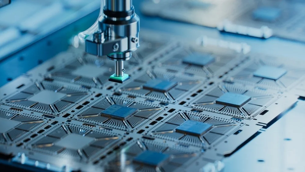
After the bare PCB has been completed, it moves to the component assembly stage to form a PCBA (Printed Circuit Board Assembly). Depending on the product structure, the production line may combine SMT, THT, soldering, dispensing, coating, potting, depaneling, and various inspection methods. This stage also offers significant opportunities for automation using dedicated machines, robots, jigs, vision systems, and control systems.
Solder paste printing and SMT component placement
SMT (Surface Mount Technology) is a technology for mounting surface-mount components directly onto PCB pads. First, solder paste is deposited onto the pads through a stencil, with the material volume controlled according to the design. The placement machine then picks up components such as resistors, capacitors, diodes, and ICs and places them at the programmed positions. The PCB then passes through a reflow oven, where the temperature is controlled according to an appropriate thermal profile to melt the solder paste and form reliable joints between the component leads or terminations and the board pads. After soldering, the board may be inspected using cameras or dedicated inspection systems before proceeding to subsequent processes. For high-volume production lines, SMT processes are typically highly automated to maintain production speed, placement accuracy, and repeatability from one production cycle to another.
Through-hole component insertion and soldering
Not all components are suitable for SMT. Large components, components requiring high mechanical strength, or components with through-hole leads, such as connectors, relays, transformers, and certain types of capacitors, may be assembled using THT (Through-Hole Technology). After the components are inserted into the board, their leads are soldered using a method appropriate to the product design and production volume. Common methods include:
Solder dipping: The PCB or component assembly is immersed in a molten solder bath to form multiple solder joints within a single cycle. This method is suitable for products whose structure and solder joint arrangement meet the requirements of solder dipping technology.
Wave soldering: The PCB is conveyed through a molten solder wave to create multiple solder joints in succession. This method is commonly suited to production lines with stable output and board designs compatible with wave soldering.
Soldering robot: A robot performs individual solder joints or soldering paths according to programmed parameters and trajectories. This approach is suitable for specialized soldering locations, applications requiring highly repeatable operations, or positions that are difficult to process using batch soldering methods.
For products with specific soldering requirements, equipment configuration should be selected based on the number of solder joints, component locations, material types, production volume, and required quality level of each product.
Dispensing, coating, and potting
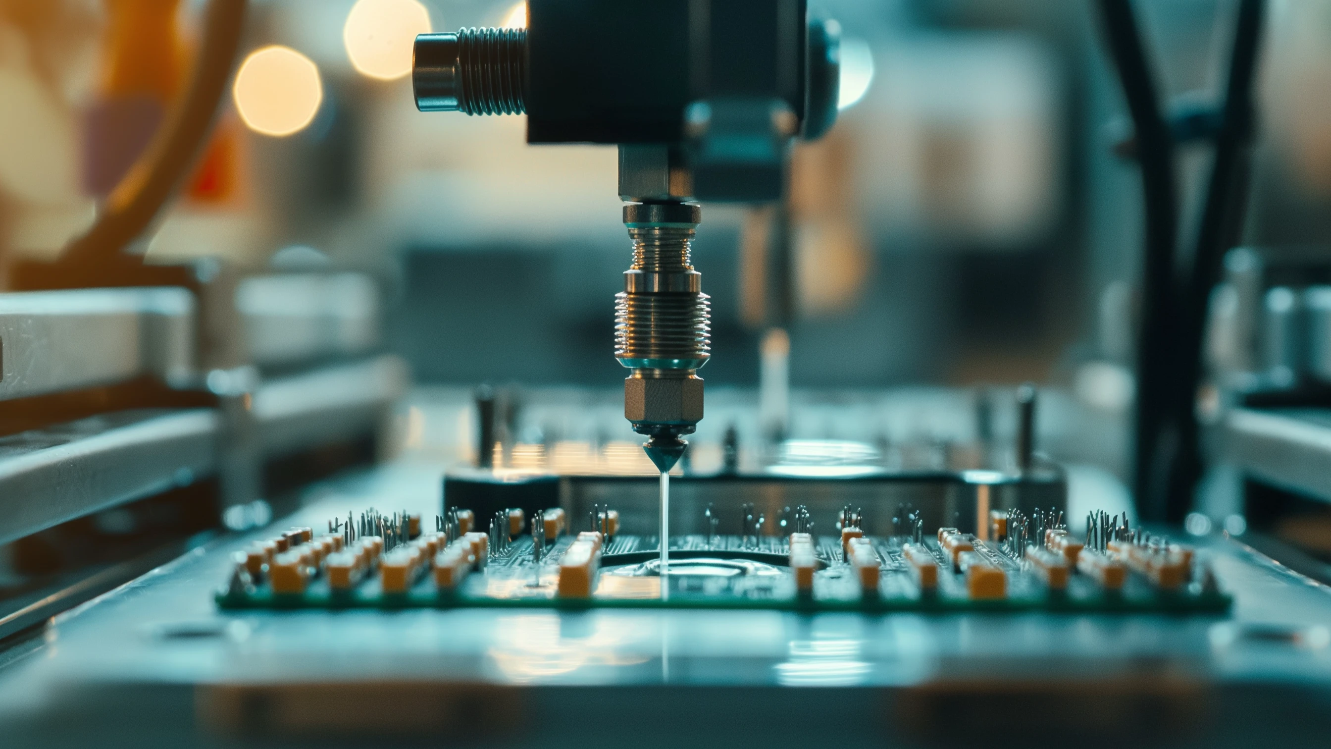
In PCBA production, adhesives and other materials may be used to secure components, protect solder joints, improve vibration resistance, prevent moisture ingress, provide electrical insulation, or protect the entire electronic assembly in demanding operating environments. Depending on the application, manufacturers may choose precision dispensing, conformal coating, or potting.
Precision dispensing
An automatic dispensing machine applies a controlled amount of material to programmed locations on the PCB. The system can control the dispensing path, movement speed, and material volume to achieve better repeatability than manual application. The accuracy of the dispensed volume and application position directly affects component retention, adhesion, and the quality of the assembly after curing. Therefore, equipment configuration should be selected based on material viscosity, dispensing point dimensions, and product requirements.
Coating
Coating applies a protective material to a defined area or surface of the circuit board. Depending on the material and coating requirements, the system may use different nozzles, flow rates, and movement paths. Automating this process helps control the coating area, material volume, and consistency between products while reducing dependence on operator technique.
Precision dispensing
A dispensing machine applies a controlled amount of material to the required location on the product. The accuracy of the material volume and dispensing position affects both component retention and the quality of the assembly after curing.
Coating
Coating applies a protective material to a defined area or surface of the circuit board. Depending on the material, the system can be configured with suitable nozzles, flow rates, and movement paths.
Potting
Potting is the process of filling or encapsulating part or all of an electronic assembly with a protective material to improve resistance to moisture and vibration, provide electrical insulation, or protect internal components. Depending on the material, curing may be performed using UV light, heat, or a specific chemical reaction. Therefore, a potting system should be designed based on the adhesive or encapsulant type, viscosity, mixing ratio where applicable, curing time, and product requirements.
Board separation and traceability marking
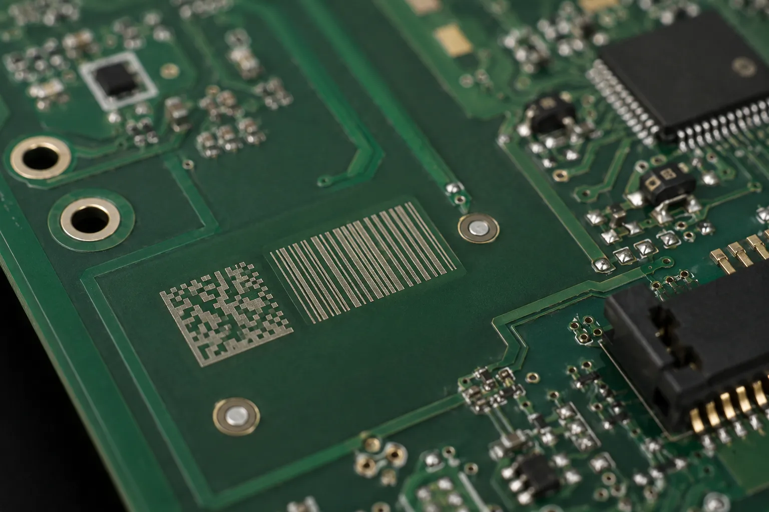
During assembly, multiple PCBs may be arranged on a single panel to facilitate material handling and simultaneous processing. After the required processes are completed, the panel can be separated into individual boards using V-cut, router, cutting blades, or laser, depending on the panel structure and product requirements. For products with components positioned close to the separation line or applications requiring high dimensional stability, the depaneling method should be selected based on the PCB material, board thickness, panel design, and component locations. In addition to board separation, lasers can be used to directly mark QR codes, serial numbers, product codes, or other traceability information onto the circuit board.
Quality inspection
Quality inspection helps identify defects before the PCBA proceeds to the next process or is incorporated into the final product. Depending on the requirements, a production line may combine multiple inspection methods:
- Visual inspection: Detects defects that can be identified by the operator or a camera system.
- AOI (Automated Optical Inspection): Uses optical systems to inspect component placement, solder joint shape, and certain assembly defects.
- ICT (In-Circuit Test): Tests electrical characteristics at designated test points on the board.
- FCT (Functional Test): Verifies the functional performance of the circuit board under predefined operating conditions.
- Continuity/short-circuit testing: Checks the electrical connectivity and identifies open or short circuits on the board.

In an automated production line, inspection data can be stored by product code to support traceability, defect analysis, and quality control.
Which PCB manufacturing processes should be automated first?
Manufacturers do not necessarily need to automate the entire production line from the outset. For factories transitioning from manual production to automation, it is generally more effective to start with processes that involve high production volumes, repetitive operations, strict accuracy requirements, or frequent defects.
| Process | Signs that automation is needed | Suitable equipment |
|---|---|---|
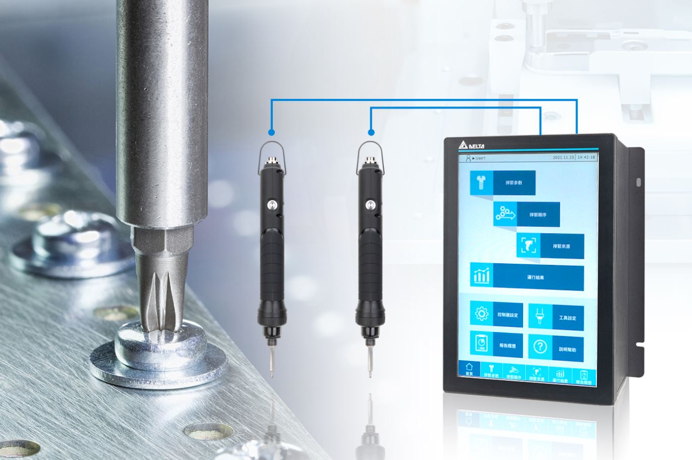
| Through-hole soldering | Recurring soldering defects, difficulty maintaining consistent quality between shifts | Automatic solder dipping machine, soldering robot |
| Dispensing | Inconsistent adhesive volume, adhesive overflow, material waste | Automatic dispensing machine |
| Coating | Inconsistent coverage, high dependence on manual operation | Automatic coating machine |
| Potting | Difficult to control material volume and dispensing position | Potting and curing system |
| Board separation | Inconsistent cut edges, potential impact on components | PCB depaneling machine |
| Traceability | Customers require a unique code for each board | Laser marking machine |
| Inspection | Manual inspection is slow and prone to missed defects | Camera, AOI, test fixture |
Prioritize high-volume processes
If an operation is repeated hundreds or thousands of times per day, automation can reduce handling time and improve production cycle consistency. Before selecting equipment, manufacturers should evaluate output per hour, cycle time, and the number of operators currently required for the process.
Prioritize processes that rely heavily on operator skill
Operations such as soldering, dispensing, and visual inspection can be significantly affected by operator experience and working conditions. For processes requiring a high degree of repeatability, automated or semi-automated equipment can provide better control over critical process parameters.
Prioritize processes requiring high accuracy
Material dispensing, soldering positions, panel separation, and code marking all require a high level of repeatability. Robots, servo systems, sensors, vision cameras, and jigs can be integrated according to the requirements of each process.
Prioritize processes requiring data traceability
When each PCB needs its own identification code, a laser marking system can be integrated with cameras or data management software to generate and verify the code before the product moves to the next process. The goal of automation is not necessarily to replace all operators. In many production lines, a more practical approach is to automate repetitive operations while operators remain responsible for material loading, equipment monitoring, inspection, and handling abnormal situations.
CNC VINA PCB production line solutions
CNC VINA designs and manufactures automation equipment and production lines for the electronics industry according to each manufacturer's requirements. Depending on the process and product characteristics, systems can be deployed as standalone machines or integrated into a complete production line.
The equipment and solutions that can be implemented include:
- Automatic solder dipping machines and PCB soldering robot systems
- Electronic component placement machines
- Dispensing and adhesive spraying machines
- PCB cutting machines
- PCB laser marking machines
- PCB inspection machines and systems
- Jigs, fixtures, and product positioning mechanisms
Equipment configuration depends not only on the machine type but also on PCB dimensions, product weight, hourly output, cycle time, component types, processing locations, inspection requirements, and available factory space.
For existing production lines, CNC VINA can evaluate individual processes to identify suitable opportunities for automation rather than requiring the entire system to be replaced. The final solution is developed based on product samples, technical requirements, and the actual operating conditions of the factory. The PCB manufacturing process begins with bare PCB fabrication and continues through component assembly processes to produce a complete PCBA. Depending on the product, the production line may include SMT, through-hole component insertion, soldering, dispensing, coating, potting, board separation, laser marking, and various inspection methods. As production volume increases or quality requirements become more stringent, repetitive processes and operations requiring high precision can be considered for automation using dedicated machines, robots, jigs, and inspection systems. CNC VINA can survey individual processes, design and manufacture dedicated equipment, or integrate multiple modules into a solution suited to the manufacturer's factory layout and production requirements. Contact CNC VINA for consultation on a PCB production line solution tailored to your actual products and production volume.
CNC VIETNAM TECHNOLOGY & APPLICATION JOINT STOCK COMPANY
Factory: Song Cung Industrial Cluster, Dong Thap Commune, Dan Phuong District, Hanoi, Vietnam.
Office: Rox Tower Goldmark City, 136 Ho Tung Mau Street, Phu Dien Ward, Hanoi, Vietnam.
Phone: +84 916 639 355 / +84 915 744 664.
Website: www.cncvina.com.vn ; www.cncvina.net