 Tiếng
Việt
 Tiếng
Anh
 Tiếng
Nhật




 Tiếng Anh

What is an acceptable solder joint? 5 inspection criteria for through-hole solder joints

7.2. PCB soldering robot
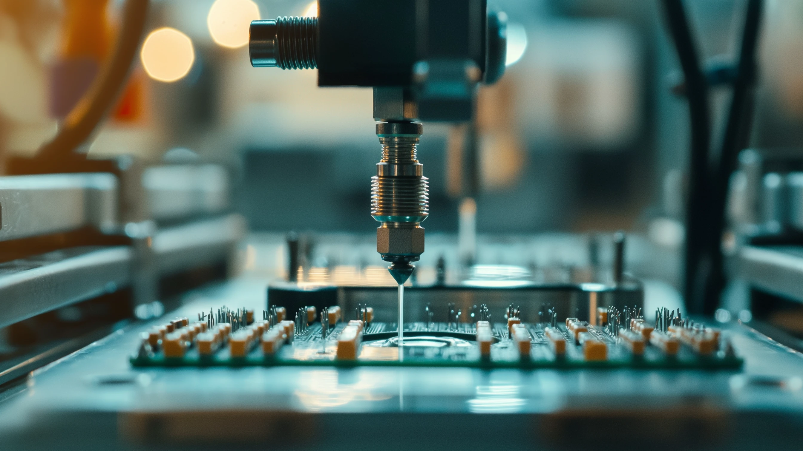
The PCB soldering robot performs soldering operations at programmed positions, making it suitable for applications requiring point-by-point soldering.
The multi-axis motion system enables controlled soldering paths, contact time, and solder feed volume. Its suitability depends on component spacing, soldering tip accessibility, and the specific quality requirements of each soldering point.
7.3. Inline flux spraying machine
The inline flux spraying machine applies flux to designated soldering areas before dip soldering or wave soldering processes.
The equipment enables controlled spray coverage, flux application volume, and consistent distribution across products. Spraying parameters are configured according to material properties, PCB structure, and actual soldering conditions.
CNC VINA can assist manufacturers in evaluating PCB samples, selecting suitable fixture designs, and establishing trial operation procedures before integrating the equipment into production.
8. Frequently asked questions about solder joint standards
8.1. Does a shiny solder joint always meet quality standards?
Not necessarily. Lead-free solder joints may have a dull surface while still meeting technical requirements. Solder joint quality must be evaluated based on wetting, joint geometry, solder coverage, and defects according to the applicable acceptance criteria.
8.2. What is the acceptable vertical hole fill percentage?
A minimum vertical hole fill of 75% is commonly used as a reference criterion for many Class 2 and Class 3 through-hole soldering applications. However, specific requirements depend on joint configuration, applicable exceptions, and the revision of the standard being used.
8.3. What is the difference between IPC-A-610 and J-STD-001?
IPC-A-610 defines acceptance criteria for electronic assemblies, while J-STD-001 specifies requirements for producing soldered electrical and electronic assemblies. These two standards are commonly used together to support manufacturing quality control and product acceptance.
8.4. Can a defective solder joint be reworked?
Yes, provided that rework is permitted under the applicable repair procedures. However, repeated heating may damage PCB pads, plated through-holes, and electronic components. Manufacturers must control rework conditions and perform appropriate inspections after soldering.
8.5. Does CNC VINA design customized soldering machines for different PCB types?
CNC VINA designs and manufactures customized automation equipment based on specific product requirements. Soldering machine configurations are evaluated according to PCB dimensions, component locations, soldering technology, production capacity, and applicable quality standards.
Solder joint standards provide manufacturers with a consistent basis for evaluating soldered connections and establishing product acceptance requirements in electronic PCB manufacturing. For through-hole solder joints, five key inspection criteria include solder wetting, vertical hole fill, joint geometry, surface condition, and component lead characteristics. Inspection results must be assessed according to the applicable product class and IPC-A-610 revision.
In addition to quality inspection, maintaining stable soldering parameters is essential for reducing defects during production. With extensive experience in automation system design and manufacturing, CNC VINA provides automatic dip soldering machines, PCB soldering robots, and flux application systems tailored to specific production requirements. These solutions help manufacturers control soldering processes, minimize operational variations, and improve product consistency.
Manufacturers can contact CNC VINA to discuss technical requirements, evaluate PCB samples, and select suitable equipment solutions for their production lines.
VIETNAM CNC AND TECHNOLOGY APPLICATION JOINT STOCK COMPANY
Factory: Song Cung Industrial Cluster, Dong Thap Commune, Dan Phuong District, Hanoi, Vietnam.
Office: Rox Tower Goldmark City, 136 Ho Tung Mau Street, Phu Dien Ward, Hanoi, Vietnam.
Phone: +84 916 639 355 / +84 915 744 664
Website: www.cncvina.com.vn ; www.cncvina.net
Email: sale01@cncvina.com.vn ; sales03@cncvina.com.vn
Join CNC VINA as we explore five key inspection criteria for through-hole solder joints based on IPC-A-610, common soldering defects, and effective solutions for solder joint quality control in PCB production lines.
1. What Is an acceptable solder joint?
An acceptable solder joint meets technical requirements for solder wetting, hole fill, joint geometry, surface condition, and component lead protrusion. It must provide reliable electrical connectivity and mechanical integrity while remaining free from defects that exceed the applicable acceptance limits. In Through-Hole Technology (THT), solder forms a connection between the component lead, plated through-hole barrel, and PCB pad. The quality of this connection depends on several factors, including solder materials, surface conditions, temperature, contact time, and soldering methods.
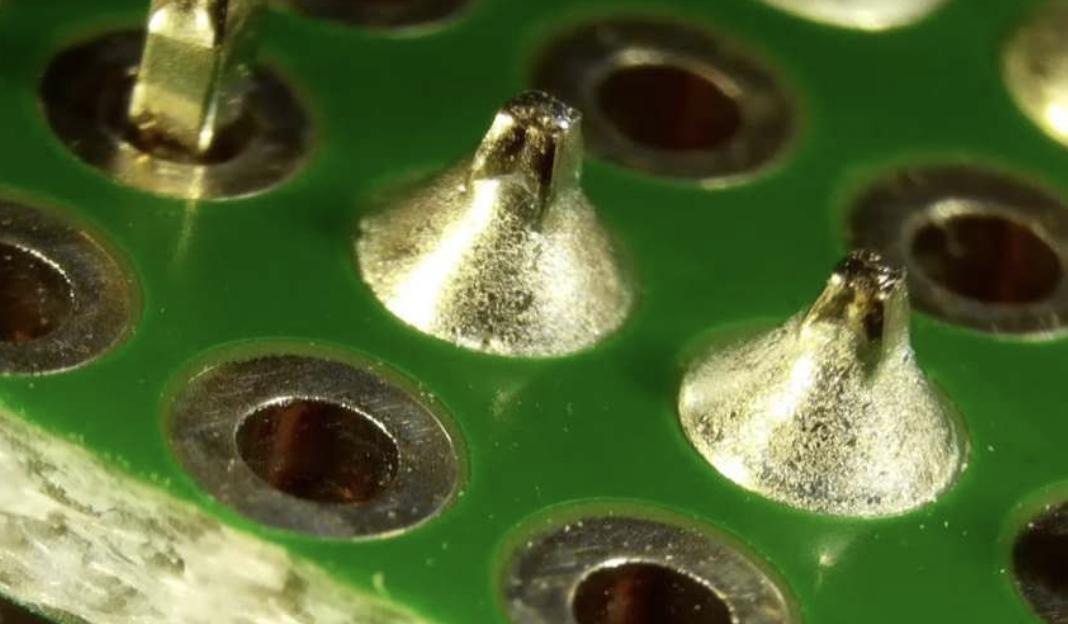
An acceptable solder joint must exhibit proper solder wetting, sufficient solder volume to establish reliable electrical and mechanical connections, appropriate joint geometry, and no defects exceeding the specified acceptance limits. Component leads and PCB pads must also meet the applicable technical requirements. Specific acceptance criteria depend on the product class, engineering drawings, and standards agreed upon with the customer.
2. IPC-A-610 standard for solder joint quality assessment
IPC-A-610 (Acceptability of Electronic Assemblies) is an industry standard that defines acceptance criteria for electronic assemblies, including solder joints, components, and assembled printed circuit boards. The IPC-A-610 standard provides a common reference for quality control (QC), quality assurance (QA), engineering teams, and customers to establish consistent inspection methods, classify defects, and determine product acceptability.
2.1. Product classification according to IPC-A-610
IPC-A-610 classifies electronic products into three categories based on their intended application and reliability requirements:
|
Product Class |
Quality Requirements |
Typical Applications |
|---|---|---|
|
Class 1 |
General electronic products designed to perform basic functions |
Electronic toys, basic consumer electronic devices |
|
Class 2 |
Products requiring reliable operation, durability, and extended service life |
Industrial equipment, power supplies, telecommunications equipment |
|
Class 3 |
High-reliability products requiring continuous performance where equipment downtime is unacceptable |
Aerospace systems, critical control systems, certain medical devices |
Class 3 generally imposes more stringent acceptance criteria. However, the applicable product class must be determined based on product characteristics, contractual specifications, and customer requirements rather than the application industry alone.
2.2. Why should manufacturers establish common standards before production?
The same solder joint may be acceptable for one product class but fail to meet the requirements of another. If manufacturers and customers apply inconsistent acceptance criteria, this can lead to product returns, additional rework costs, and quality-related complaints. Before production begins, manufacturers should clearly define the applicable product class (Class 1, 2, or 3), IPC-A-610 revision, engineering drawing requirements, inspection methods, and procedures for handling nonconforming products. Establishing these requirements in advance helps maintain consistent quality across production batches and shifts.
3. Five key inspection criteria for acceptable through-hole solder joints
To assess the quality of through-hole solder joints, QC personnel must inspect solder wetting, vertical hole fill, joint geometry, and other relevant technical characteristics. The following criteria are essential for evaluating solder joint quality in PCB manufacturing.
3.1. Solder wettability
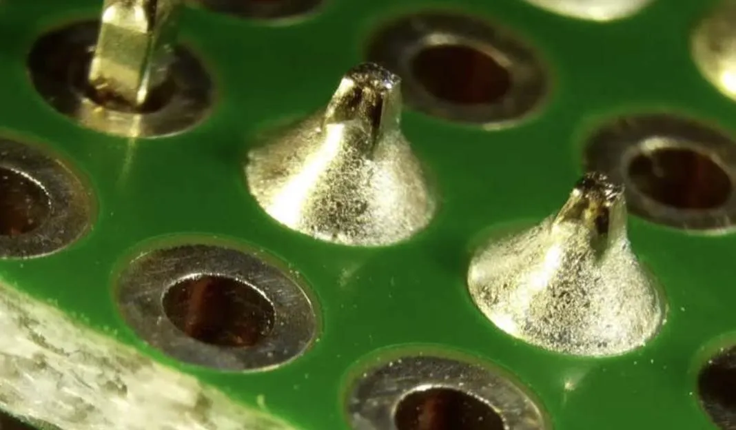
Solder wetting refers to the ability of molten solder to spread across and adhere to component leads, PCB pads, or plated through-hole barrels. A properly wetted solder joint typically exhibits continuous contact areas and smooth transitions, without solder balling up or separating from the surfaces being joined. During inspection, particular attention should be paid to solder adhesion, the geometry of wetted areas, and any signs of nonwetting or dewetting that exceed the specified acceptance limits. A contact angle of less than 90° is commonly used as a reference indicator of solder wettability. However, it should not be considered the sole criterion for determining solder joint acceptability.
Poor wetting is commonly caused by surface oxidation, contamination, unsuitable flux, or insufficient soldering temperature.
3.2. Vertical hole fill
Vertical hole fill refers to the percentage of the plated through-hole height filled with solder in the space between the component lead and the plated hole barrel, relative to the PCB thickness. For many conventional through-hole soldering applications, a minimum vertical fill of 75% is used as a reference acceptance criterion for Class 2 and Class 3 products. However, specific requirements depend on hole configuration, component type, and applicable exceptions defined in IPC-A-610. Insufficient hole fill can reduce the effective bonding area, mechanical strength, and resistance to vibration. Common causes include inadequate heat transfer, surface oxidation, unsuitable flux, improper hole dimensions, or insufficient soldering contact time.
For high-reliability products, manufacturers may combine visual inspection with cross-sectional analysis to verify solder fill within plated through-holes.
3.3. Solder Joint Geometry and Solder Volume
Solder joint geometry reflects the quality of solder wetting and the distribution of solder around component leads. On the solder side of the PCB, solder must form an appropriate connection between the component lead and pad, without insufficient solder or excessive accumulation beyond the specified acceptance limits. During inspection, QC personnel should evaluate joint geometry, solder volume, solder coverage, and the visibility of critical bonding areas. Excessive solder may obscure inspection areas or cause solder bridging, while insufficient solder can reduce the bonding area and mechanical strength. Solder joint geometry must be assessed according to the specific component lead configuration, PCB pad design, and corresponding IPC-A-610 acceptance criteria. A single joint shape should not be applied as a universal requirement for all solder connections.
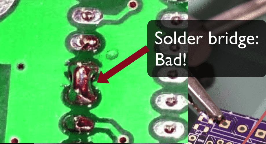
During inspection, particular attention should be paid to the following aspects:
-
Whether the solder joint geometry is appropriate for the component lead and pad configuration.
-
Whether the solder volume meets the requirements for coverage and joint integrity.
-
Whether unintended solder bridges have formed between conductive areas.
-
Whether excess solder obscures critical features required for quality assessment.
Excessive solder may make it difficult to evaluate wetting conditions and increase the risk of solder bridging between closely spaced component leads. Conversely, insufficient solder may fail to meet the requirements for solder coverage, vertical hole fill, or mechanical integrity. It is important to note that a concave solder fillet is not a universal requirement for all component lead configurations. Solder joint acceptability must be evaluated based on lead geometry, pad structure, and the applicable criteria specified in the standard.
3.4. Solder joint surface condition
The solder joint surface is one of the first characteristics examined during visual inspection.
An acceptable solder joint should exhibit a continuous bonded surface without unacceptable defects such as cracks or signs of joint separation. However, solder joint quality cannot be determined solely by surface brightness or gloss.
|
Characteristics |
Leaded solder |
Lead-free solder |
|---|---|---|
|
Typical surface appearance |
Relatively bright and smooth |
May appear dull or grainy |
|
Surface gloss |
Generally higher |
May be lower |
|
Evaluation method |
Assess joint geometry, wetting, and defects together |
Do not classify a joint as defective solely because of a dull surface |
Potential defects to inspect include cracks, voids, pinholes, abnormal surface conditions, and signs of solder joint disturbance during solidification. Not all pinholes or surface irregularities automatically require product rejection. Acceptability must be determined based on the characteristics of the defect and the applicable inspection standard.
3.5. Component lead length and condition
In addition to the solder itself, component leads must be inspected to ensure mechanical integrity and adequate clearance from surrounding components and conductive surfaces. Key inspection points include lead protrusion length, lead trimming condition, mechanical deformation, visibility of lead ends, and clearance from adjacent conductive surfaces. Excessively long leads may reduce electrical clearance, while improper lead trimming can introduce mechanical stress or damage PCB pads. Acceptance limits must be verified according to the specific component lead configuration and the corresponding requirements of IPC-A-610.
4. Common PCB soldering defects and how to identify them
During through-hole soldering, solder joint quality is influenced by several factors, including soldering materials, PCB design, solder bath temperature, flux application, and contact time. Accurate identification of common PCB soldering defects enables QC personnel to determine potential causes and make timely adjustments to the manufacturing process.

|
Defect type |
Identifying characteristics |
Common causes |
|---|---|---|
|
Cold solder joint |
Poor bonding, abnormal surface appearance, or visible cracks |
Insufficient heat, poor wetting, movement during solidification |
|
Insufficient solder |
Inadequate solder coverage or vertical hole fill |
Insufficient flux, low temperature, short contact time |
|
Excessive solder |
Excessive solder accumulation obscuring inspection areas |
Improper soldering parameters or inadequate solder drainage |
|
Solder bridging |
Unintended solder connections between conductive areas |
Narrow lead spacing, poor solder drainage |
|
Voids and pinholes |
Cavities on the surface or inside solder joints |
Moisture, gas release during soldering, improper heating conditions |
|
Nonwetting |
Solder fails to spread across or adhere to the surface |
Oxidation, contamination, unsuitable flux |
4.1. Cold solder joints and nonwetting
Cold solder joints are commonly associated with inadequate thermal conditions or improper solidification. In contrast, nonwetting occurs when solder fails to form a proper metallurgical bond with the surface being soldered. Although these defects may exhibit similar visual characteristics, their underlying causes can differ. When such defects are detected, manufacturers should inspect component lead surfaces, PCB pads, flux activity, and soldering temperature parameters. A dull or gray appearance on lead-free solder joints alone should not be considered sufficient evidence of a cold solder joint.
4.2. Solder bridging between component leads
Solder bridging occurs when solder unintentionally connects conductive areas that should remain electrically isolated. This defect commonly appears in areas with narrow lead spacing or where solder drainage is unstable. In dip soldering and wave soldering processes, key parameters to inspect include solder bath temperature, flux application, contact time, component orientation, and PCB withdrawal speed. Solder bridges that cause electrical short circuits must be corrected before final product acceptance.
4.3. Voids and pinholes in solder joints
Voids form when gas becomes trapped in molten solder or is released during solidification. Potential causes include moisture in PCBs, components, or soldering materials, as well as unsuitable heating conditions. Some surface voids can be detected through visual inspection, while internal defects require appropriate inspection methods. QC personnel must assess the size, location, and potential impact of these defects on joint integrity according to the applicable acceptance criteria.
5. Solder joint quality inspection methods in manufacturing
Solder joint inspection helps identify defects before assembled PCBs proceed to subsequent production stages. Depending on production volume and quality requirements, manufacturers can adopt the following inspection methods.
5.1. Visual inspection using magnification
QC personnel use direct visual observation, magnifying glasses, or stereo microscopes to assess solder wetting, joint geometry, solder coverage, and surface defects. Inspection areas should be equipped with appropriate lighting, standardized operating instructions, and reference images illustrating acceptable and unacceptable conditions for each product class. Magnification levels should be selected according to specific inspection requirements.
5.2. Automated optical inspection (AOI)
Automated optical inspection (AOI) uses cameras and image-processing algorithms to detect abnormalities such as insufficient solder, solder bridging, irregular solder joint geometry, and component misalignment, depending on the equipment configuration. This method is suitable for high-volume production lines and helps maintain inspection consistency. However, AOI cannot fully evaluate internal defects within plated through-holes or areas obscured from camera view.
5.3. Solder joint cross-sectional inspection
Cross-sectional analysis enables manufacturers to examine joint structure, vertical solder fill, and internal defects within plated through-holes. As this is a destructive inspection method, it is typically used for process validation, failure analysis, or sample testing according to established quality control plans.
5.4. Electrical and functional testing of PCBs
Testing methods such as in-circuit testing (ICT) and functional circuit testing (FCT) help detect open circuits, short circuits, and functional abnormalities. However, passing electrical tests does not necessarily mean that a product fully complies with IPC-A-610 acceptance criteria. Therefore, manufacturers should combine functional testing with visual inspection and other appropriate quality assessment methods. For further information, refer to the PCB manufacturing process to understand the role of soldering and inspection in PCB production lines.
6. The role of automated soldering equipment in solder joint quality control
In high-volume PCB manufacturing, solder joint quality depends on maintaining consistent temperature, contact time, positioning, and solder volume. Compared with manual operations, automated soldering equipment enables manufacturers to control process parameters through programmed settings, reducing variations between production cycles.
6.1. Control of soldering temperature and contact time
Soldering temperature and contact time influence heat transfer, flux activation, and solder wetting. Insufficient heat may result in inadequate solder fill or poor bonding, while excessive temperatures or prolonged contact can increase the risk of damage to PCB pads and electronic components. Automated soldering machines allow operating parameters to be programmed and consistently repeated. These settings must be validated using actual products before mass production.
6.2. Maintaining positioning and contact conditions
In dip soldering, immersion depth, dwell time, and PCB withdrawal speed directly influence the amount of solder deposited on component leads. Motion control systems combined with dedicated fixtures help maintain consistent product positioning and minimize operational variations. In robotic soldering applications, programmable control systems enable precise positioning, contact time adjustment, and solder feeding at individual soldering points, depending on the equipment configuration.
6.3. Supporting multiple PCB models
Automated soldering equipment with program storage capabilities helps reduce setup time when switching between previously validated PCB models. When PCB designs, components, or materials change, manufacturers must still revalidate the corresponding soldering conditions. Systems equipped with data logging functions can also support the traceability of operating parameters by production batch. Although automation improves process consistency, solder joint quality remains dependent on PCB design, materials, fixtures, and soldering programs.
7. PCB soldering equipment solutions from CNC VINA
With extensive experience in designing and manufacturing automation systems, CNC VINA provides equipment solutions for electronic PCB soldering processes. Each solution is selected and configured according to PCB structure, soldering method, production capacity, and the specific quality requirements of the manufacturer.
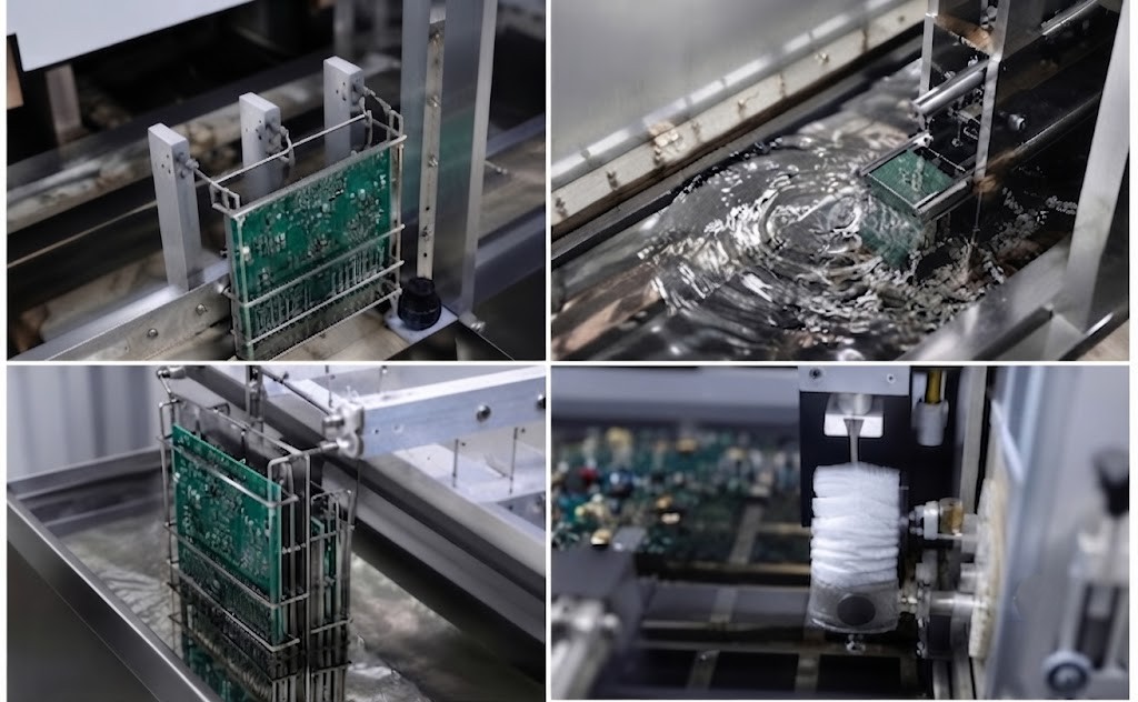
7.1. Automatic dip soldering machine
The automatic dip soldering machine is designed for dip soldering suitable areas of printed circuit boards. Depending on its configuration, the equipment can control immersion movement, contact time, and product withdrawal. Dedicated fixtures are designed according to PCB dimensions, component lead positions, and areas requiring protection. Maintaining consistent dipping conditions helps minimize operational variations between production cycles.
7.2. PCB soldering robot
The PCB soldering robot performs soldering operations at programmed positions, making it suitable for applications requiring point-by-point soldering.
The multi-axis motion system enables controlled soldering paths, contact time, and solder feed volume. Its suitability depends on component spacing, soldering tip accessibility, and the specific quality requirements of each soldering point.
7.3. Inline flux spraying machine
The inline flux spraying machine applies flux to designated soldering areas before dip soldering or wave soldering processes. The equipment enables controlled spray coverage, flux application volume, and consistent distribution across products. Spraying parameters are configured according to material properties, PCB structure, and actual soldering conditions. CNC VINA can assist manufacturers in evaluating PCB samples, selecting suitable fixture designs, and establishing trial operation procedures before integrating the equipment into production.
8. Frequently asked questions about solder joint standards
8.1. Does a shiny solder joint always meet quality standards?
Not necessarily. Lead-free solder joints may have a dull surface while still meeting technical requirements. Solder joint quality must be evaluated based on wetting, joint geometry, solder coverage, and defects according to the applicable acceptance criteria.
8.2. What is the acceptable vertical hole fill percentage?
A minimum vertical hole fill of 75% is commonly used as a reference criterion for many Class 2 and Class 3 through-hole soldering applications. However, specific requirements depend on joint configuration, applicable exceptions, and the revision of the standard being used.
8.3. What is the difference between IPC-A-610 and J-STD-001?
IPC-A-610 defines acceptance criteria for electronic assemblies, while J-STD-001 specifies requirements for producing soldered electrical and electronic assemblies. These two standards are commonly used together to support manufacturing quality control and product acceptance.
8.4. Can a defective solder joint be reworked?
Yes, provided that rework is permitted under the applicable repair procedures. However, repeated heating may damage PCB pads, plated through-holes, and electronic components. Manufacturers must control rework conditions and perform appropriate inspections after soldering.
8.5. Does CNC VINA design customized soldering machines for different PCB types?
CNC VINA designs and manufactures customized automation equipment based on specific product requirements. Soldering machine configurations are evaluated according to PCB dimensions, component locations, soldering technology, production capacity, and applicable quality standards. Solder joint standards provide manufacturers with a consistent basis for evaluating soldered connections and establishing product acceptance requirements in electronic PCB manufacturing. For through-hole solder joints, five key inspection criteria include solder wetting, vertical hole fill, joint geometry, surface condition, and component lead characteristics. Inspection results must be assessed according to the applicable product class and IPC-A-610 revision.
In addition to quality inspection, maintaining stable soldering parameters is essential for reducing defects during production. With extensive experience in automation system design and manufacturing, CNC VINA provides automatic dip soldering machines, PCB soldering robots, and flux application systems tailored to specific production requirements. These solutions help manufacturers control soldering processes, minimize operational variations, and improve product consistency.
Manufacturers can contact CNC VINA to discuss technical requirements, evaluate PCB samples, and select suitable equipment solutions for their production lines.
VIETNAM CNC AND TECHNOLOGY APPLICATION JOINT STOCK COMPANY
Factory: Song Cung Industrial Cluster, Dong Thap Commune, Dan Phuong District, Hanoi, Vietnam.
Office: Rox Tower Goldmark City, 136 Ho Tung Mau Street, Phu Dien Ward, Hanoi, Vietnam.
Phone: +84 916 639 355 / +84 915 744 664
Website: www.cncvina.com.vn ; www.cncvina.net
Email: sale01@cncvina.com.vn ; sales03@cncvina.com.vn