 Tiếng
Việt
Tiếng
Việt
 Tiếng
Anh
Tiếng
Anh
 Tiếng
Nhật
Tiếng
Nhật




 Tiếng Anh

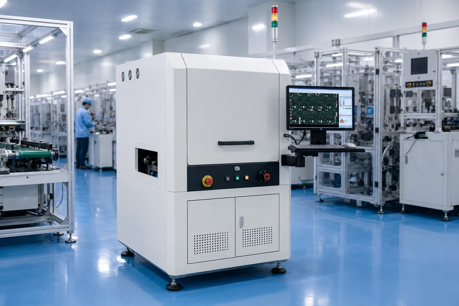
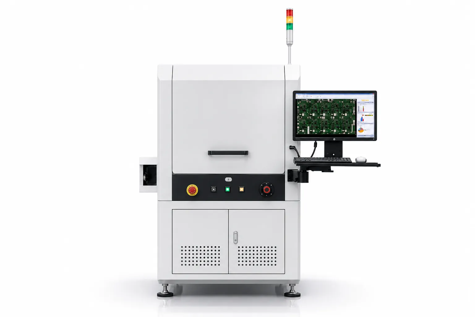
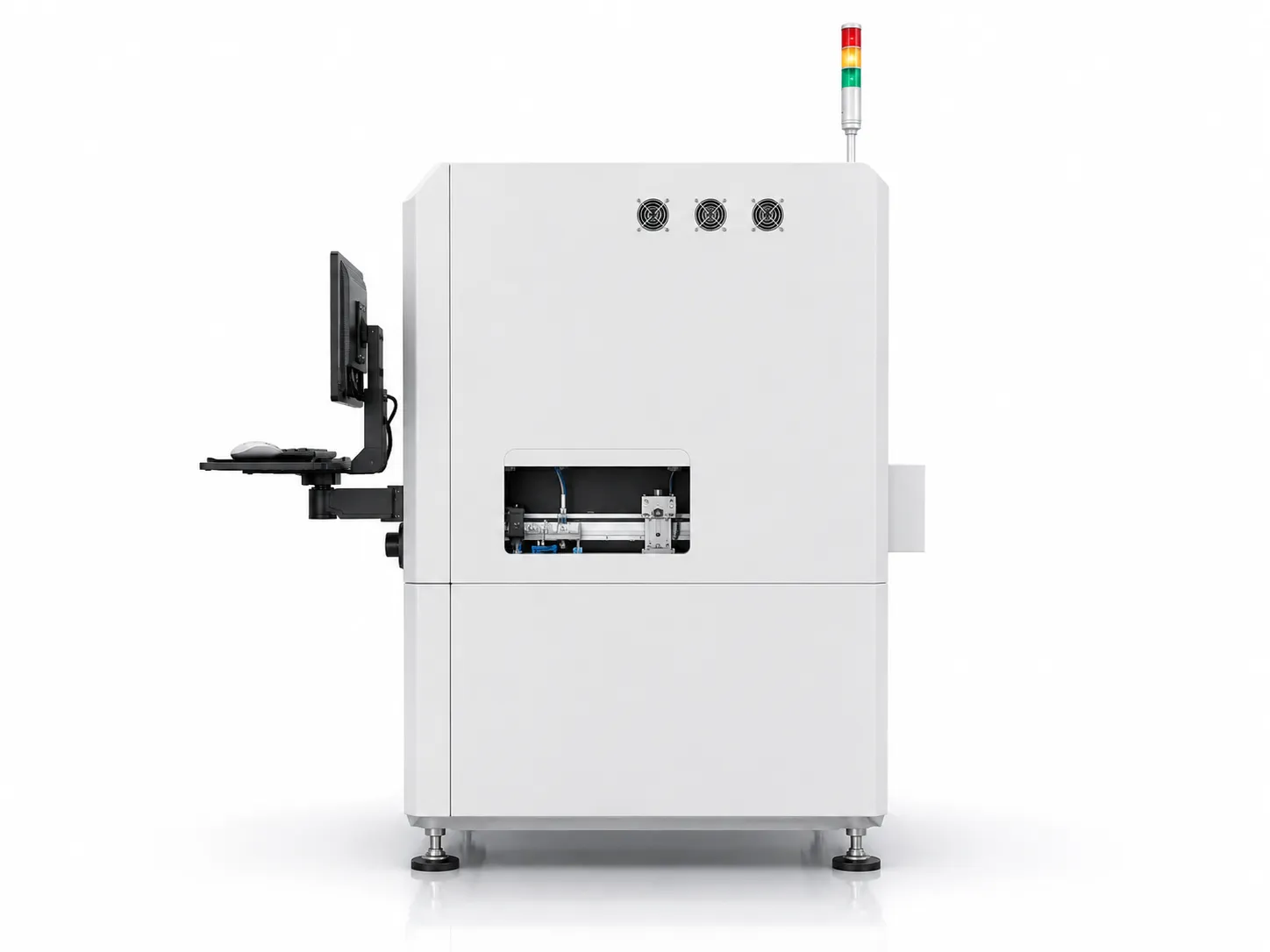
Automatic PCB Inspection Machine
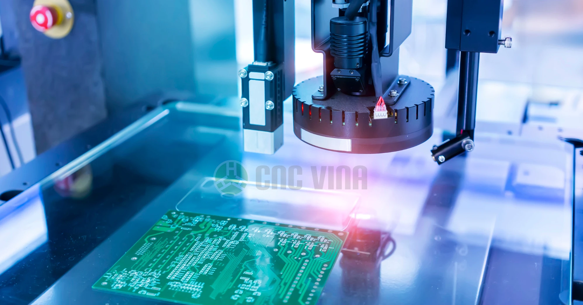
Automatic PCB Inspection Machine is an automated optical inspection system designed to detect defects on printed circuit boards (PCBs) throughout the manufacturing process. The machine uses high-resolution industrial cameras combined with advanced image-processing algorithms to scan the entire PCB surface and identify defects related to components, solder joints, assembly positions, and other manufacturing irregularities that can be difficult to detect through manual inspection.
As electronic products become increasingly compact and sophisticated, PCBs are being designed with higher component densities, smaller components, and increasingly complex multilayer structures. A single PCB may contain thousands of electronic components, with extremely small distances between component pins and solder joints. Under these conditions, manual inspection is not only time-consuming but also highly dependent on the operator’s experience and concentration. This can lead to inconsistent inspection results and an increased risk of human error, particularly in high-volume production environments.
The Automatic PCB Inspection Machine is developed to automate the PCB quality inspection process, enabling manufacturers to identify defects directly on the production line. By combining high-resolution imaging technology with intelligent image analysis, the system can inspect PCBs quickly and consistently, helping reduce defective products, improve production efficiency, and maintain stable quality across large production volumes.
For manufacturers looking to improve production automation, inspection accuracy, and quality control, an automatic PCB inspection system provides an effective solution for detecting manufacturing defects at an early stage. By identifying potential problems before the PCB moves to subsequent processes, the machine helps reduce rework and production losses while supporting a more reliable and efficient electronics manufacturing process.
VIETNAM CNC & TECHNOLOGY APPLICATION JOINT STOCK COMPANY
Hotline: +84.916 63 9355 / +84.915 74 4664
Email: Sales01@cncvina.com.vn / Sales03@cncvina.com.vn
Product description

An Automatic PCB Inspection Machine is an automated optical inspection system designed to detect defects on printed circuit boards (PCBs) throughout the manufacturing process. The machine uses high-resolution industrial cameras combined with advanced image-processing algorithms to scan the entire PCB surface and identify defects related to components, solder joints, assembly positions, and other manufacturing irregularities that can be difficult to detect through manual inspection. As electronic products become increasingly compact and sophisticated, PCBs are being designed with higher component densities, smaller components, and increasingly complex multilayer structures. A single PCB may contain thousands of electronic components, with extremely small distances between component pins and solder joints. Under these conditions, manual inspection is not only time-consuming but also highly dependent on the operator’s experience and concentration. This can lead to inconsistent inspection results and an increased risk of human error, particularly in high-volume production environments. The Automatic PCB Inspection Machine is developed to automate the PCB quality inspection process, enabling manufacturers to identify defects directly on the production line. By combining high-resolution imaging technology with intelligent image analysis, the system can inspect PCBs quickly and consistently, helping reduce defective products, improve production efficiency, and maintain stable quality across large production volumes.
For manufacturers looking to improve production automation, inspection accuracy, and quality control, an automatic PCB inspection system provides an effective solution for detecting manufacturing defects at an early stage. By identifying potential problems before the PCB moves to subsequent processes, the machine helps reduce rework and production losses while supporting a more reliable and efficient electronics manufacturing process.
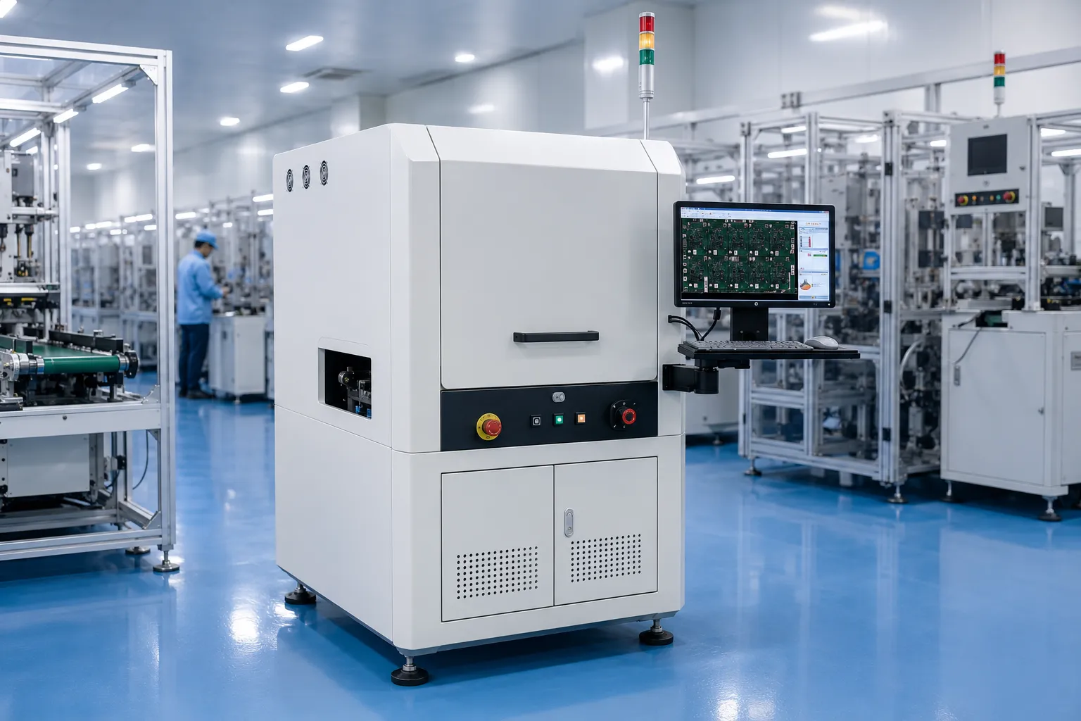
Technical specifications and structure of the PCB inspection machine
Technical specifications
| Dimensions | L1200 x W1000 x H1800 mm |
| Power | 2kW |
| Power supply | Single - phase 220V - 50Hz |
| Control voltage | DC 24V |
| Air supply Requirement | 0.4 -0.6 MPa |
| Model | HV, GAS |
| Max PCB size | L250 x W120 x H3 mm |
| Cycle time | 5 - 14 seconds |
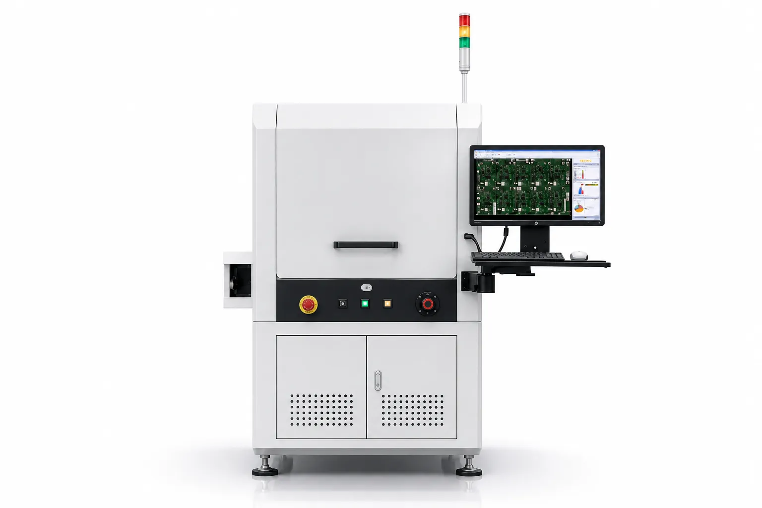
Basic Configuration of the PCB Inspection Machine
Loading & Unloading Conveyor: The conveyor automatically transfers PCBs into and out of the inspection area. The distance between the guide rails can be adjusted to accommodate different PCB sizes, allowing the machine to be easily integrated into existing SMT production lines.
PCB Positioning Jig: The positioning jig securely holds the PCB throughout the inspection process to minimize vibration and movement. This ensures that the camera consistently captures images at the correct position, maintaining high inspection accuracy.
Industrial Camera System: The industrial camera system is the most critical component of an AOI machine. High-resolution cameras combined with specialized lenses capture even the smallest details on the PCB surface. Depending on the application, the machine can be equipped with one or multiple cameras to increase inspection speed and coverage.
Lighting System: A multi-angle LED lighting system with different light colors enhances the visibility of components and solder joints, enabling the camera system to identify defects more accurately across different materials and surface conditions.
Image Processing Software: The software performs the following functions:
- Comparison with reference data
- Image analysis
- Defect detection
- Defect location marking
- Inspection data storage
- Defect rate statistics
- Production history traceability
Many modern AOI systems can also integrate Artificial Intelligence (AI) technology to reduce the false call rate and improve inspection accuracy.
Sensor System: Sensors accurately detect the position of each PCB, control the machine operating sequence, and ensure stable and consistent inspection throughout the production process.
OK/NG Sorting Trays: After inspection, qualified PCBs are automatically transferred to the OK tray, while defective PCBs are directed to the NG tray for further inspection, troubleshooting, or repair by technicians.
How the PCB Inspection Machine Works
The PCB Inspection Machine operates based on image acquisition and software-based data processing. Once a PCB enters the machine through the conveyor system, it is precisely positioned using the positioning jig and sensors. The specialized LED lighting system illuminates the PCB surface at an appropriate intensity, allowing the industrial cameras to capture each area of the board at very high resolution. The captured images are then analyzed by the image processing software and compared with reference data, such as a Golden Board or CAD/Gerber data. When a deviation is detected, the system automatically identifies the defect location, classifies the defect, and provides an OK or NG inspection result. With high-speed image processing capabilities, the machine can inspect thousands of points on a single PCB within just a few seconds while maintaining a high level of inspection accuracy.
Defects Detectable by the PCB Inspection Machine
The PCB Inspection Machine can detect most common defects occurring during the PCB assembly process, including:
- Missing components
- Incorrect components
- Component misalignment
- Incorrect component orientation
- Incorrect component polarity
- Incorrect component value
- Solder bridges
- Insufficient solder
- Cold solder joints
- Open circuits
- Defective solder joints
- Bent IC leads
- Cracked or damaged components
- Foreign objects or contaminants on the PCB
- Scratches on PCB traces
- Incorrect solder joint size or shape
Fast and accurate defect detection significantly reduces the risk of defective PCBs passing through the production line and reaching subsequent processes or customers.
Advantages of the PCB Inspection Machine
Improved Product Quality
The AOI PCB Inspection Machine detects defects at an early stage of the PCB assembly process, before the product moves to subsequent manufacturing stages or is shipped to customers. Automated inspection with high accuracy allows non-conforming PCBs to be identified directly on the production line, reducing the risk of defective products reaching customers.
In addition, the machine helps maintain consistent quality across different production batches. Every PCB is inspected according to the same predefined standards, reducing variations caused by manual inspection and improving overall product consistency.
High Inspection Accuracy
The PCB Inspection Machine combines high-resolution industrial cameras, a specialized lighting system, and advanced image-processing algorithms to inspect individual details across the PCB surface. The system can identify small defects such as missing components, component misalignment, incorrect polarity, solder bridges, insufficient solder, and surface defects that may be difficult for human operators to detect.
High inspection accuracy not only helps reduce the defect rate but also minimizes missed defects and false calls, contributing to more effective quality control in modern SMT production lines.
Fully Automated Inspection Process
The entire inspection process is performed automatically according to the programmed inspection parameters. Once a PCB enters the machine, the system automatically positions the board, captures images, analyzes the data, compares the results against predefined standards, and provides the final inspection result without requiring continuous operator intervention. Automation reduces dependence on manual labor, minimizes errors caused by human factors, and maintains consistent inspection performance even during continuous long-term production.
Increased Production Productivity
With a fast inspection cycle of only 5–14 seconds, the PCB Inspection Machine can meet the requirements of high-speed SMT production lines without affecting production throughput. Compared with manual inspection, the machine significantly reduces inspection time and increases the number of PCBs that can be processed within the same production period. Early defect detection on the production line also reduces repair time at subsequent stages, minimizes production downtime and rework, and improves the overall efficiency of the manufacturing line.
Reduced Manufacturing Costs
The cost of correcting defects after a product has been completed or delivered to customers is often significantly higher than identifying those defects during production. An AOI system enables manufacturers to detect assembly defects at an early stage, helping reduce scrap rates, repair costs, product returns, and warranty-related expenses. By reducing the number of defective products, the system also helps manufacturers save materials, labor, and production time, contributing to lower overall operating costs in the long term.
Inspection Data Traceability and Quality Management
The AOI system can store inspection data, including inspection images, defect locations, defect types, and inspection results for individual PCBs. This information allows manufacturers to quickly retrieve inspection records when analyzing the root causes of defects or evaluating production line performance. Through statistical reports, engineering teams can identify where defects occur in the production process, implement corrective actions, optimize manufacturing processes, and improve product quality in subsequent production batches.
Support for Electronics Manufacturing Standards
For industries such as consumer electronics, automotive, medical devices, and aerospace, PCB quality must meet strict manufacturing and quality requirements. The PCB Inspection Machine supports quality control processes aligned with standards such as IPC and RoHS, as well as other applicable technical requirements. Compliance with these standards not only helps manufacturers improve product quality and credibility but also supports their ability to supply products to major manufacturers and expand into international markets.
Other PCB Inspection Methods
In addition to Automated Optical Inspection (AOI), electronics manufacturers use various inspection methods to evaluate PCB quality at different stages of production. Each method has its own operating principle and application range, so many factories combine multiple inspection technologies to establish a comprehensive quality control process.
Visual Inspection
Visual inspection uses the naked eye or optical aids such as magnifying glasses and microscopes to examine the PCB surface and identify defects such as missing components, incorrect component placement, or defective solder joints. This method has a relatively low implementation cost but depends heavily on the inspector's experience and attention. It is generally less suitable for PCBs with high component density or large-scale production.
Manual Electrical Testing
Manual testing uses a multimeter or other electrical measurement equipment to check circuit continuity, detect short circuits, open circuits, or incorrect voltage levels. This method is commonly used for troubleshooting, repair, or prototype testing but is generally not suitable for high-volume production.
Automated X-ray Inspection (AXI)
AXI (Automated X-ray Inspection) uses X-ray technology to inspect internal PCB structures that cannot be observed using conventional cameras. It is particularly effective for inspecting solder joints beneath BGA, CSP, and QFN components, as well as multilayer PCBs. Because AXI can visualize internal structures and hidden solder joints, it can detect defects such as voids, insufficient solder, open solder joints, and other hidden defects that may not be detectable by AOI. However, the initial investment cost of an AXI system is generally higher than that of an AOI system.
In-Circuit Test (ICT)
ICT (In-Circuit Test) checks individual components on a PCB using specialized probes that make direct contact with designated test points on the board. The system measures the electrical characteristics of individual components, such as resistors, capacitors, diodes, transistors, and integrated circuits, to determine whether they meet the designed specifications. ICT can quickly identify component and electrical connection defects. However, it requires a dedicated test fixture for each PCB type, which can result in relatively high implementation costs.
Functional Circuit Test (FCT)
FCT (Functional Circuit Test) evaluates the actual operating performance of a PCB after the assembly process has been completed. During the test, the PCB is powered and operated under conditions similar to its actual application. The system can evaluate functions, input/output signals, communication capabilities, power consumption, and overall operating performance. FCT helps verify that the complete system operates according to the design requirements while identifying functional defects that may not be detected by other inspection methods.
Burn-in Testing
Burn-in testing involves operating a PCB continuously under elevated temperature or load conditions to identify potential reliability issues and latent defects. This method is commonly applied to products requiring a high level of reliability, including medical devices, automotive electronics, and industrial electronic equipment.
CNC VINA – Customized PCB Inspection Machine Supplier
CNC VINA specializes in the design, manufacturing, and integration of automation systems for the electronics manufacturing industry. The PCB Inspection Machine from CNC VINA is designed to meet specific production requirements and can be directly integrated into existing production lines, helping manufacturers improve quality control efficiency and optimize production performance.
The engineering team at CNC VINA provides comprehensive support, including solution consulting, customized machine design based on actual product requirements, installation, operator training, and after-sales maintenance. These services enable CNC VINA to deliver tailored automation solutions for electronics manufacturers in both domestic and international markets.
If you are looking for an automated PCB inspection solution tailored to your production requirements, please contact us for consultation:
Vietnam CNC & Technology Application Joint Stock Company
Factory: Song Cung Industrial Point, Dong Thap Commune, Dan Phuong District, Hanoi, Vietnam
Phone: +84.916 63 9355 / +84.915 74 4664
Website: https://cncvina.com.vn; https://cncvina.net; https://cncviname.com.vn
Email: sales01@cncvina.com.vn